Huawei is reportedly advancing its chipmaking capabilities significantly, with sources indicating the development of two distinct types of 3nm chips. This ambitious undertaking aims to push the boundaries of semiconductor technology within China, even as the company faces extensive international sanctions that restrict access to advanced manufacturing equipment, particularly EUV lithography machines from ASML.
According to reports, Huawei is pursuing a dual-track strategy for its 3nm development. One approach focuses on Gate-All-Around (GAA) FET technology, a next-generation transistor architecture that promises improved power efficiency and performance. The other involves exploring futuristic carbon nanotube-based semiconductors, a potentially revolutionary technology though its current progress remains largely undisclosed.
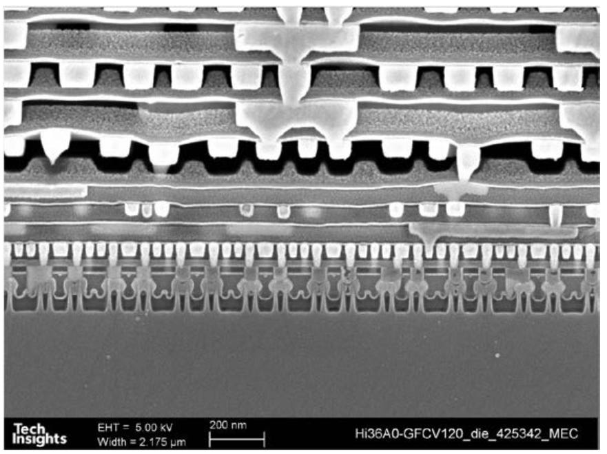
This push toward 3nm follows Huawei’s recent success with the 5nm Kirin X90 chip. Despite not having access to ASML’s EUV machines, the company, in partnership with SMIC, utilized Deep Ultraviolet (DUV) lithography combined with complex multi-patterning techniques to manufacture the 5nm chip. While a notable achievement under the circumstances, this method resulted in a reported yield of only 20%, significantly lower than industry standards for mature nodes.


The 3nm GAA FET chip is reportedly slated for a tape-out in 2026. If development proceeds as planned and yields improve, mass production could potentially begin in 2027. However, relying on DUV lithography for the even tighter tolerances of a 3nm process is expected to lead to even lower yields than seen with the 5nm chips, posing significant cost and manufacturing challenges.
To overcome these hurdles, Huawei has reportedly invested heavily, committing $37 billion towards the development of domestic EUV technology. Some insiders are optimistic that China’s own EUV capabilities could be operational by 2026. Despite this optimism, experts, including former ASML engineers, remain skeptical about China’s near-term ability to replicate ASML’s sophisticated EUV technology, which took decades to perfect.
Huawei has maintained a veil of secrecy around its progress in advanced manufacturing and EUV development, similar to the approach taken with the rollout of its Kirin 9010 processor. Should Huawei successfully navigate the complexities of producing 3nm chips using GAA technology, and potentially carbon nanotubes in the future, it could significantly narrow the technological gap with global leaders like TSMC and Samsung, who currently dominate the 3nm space using EUV lithography. The success of this endeavor could redefine China’s position in the global semiconductor landscape, though the challenges of low yields and DUV dependency remain substantial obstacles.