Intel is set to unveil its groundbreaking “Meteor Lake” processors, representing a departure from the previous 14th Gen Core series. These processors will debut on consumer laptops, prioritizing efficiency and extended battery life. While specific details on chip models and performance remain under wraps, Intel has provided a broad view of the innovations behind Meteor Lake.
This includes revamped chip designs, updated technology, and enhanced features aimed at boosting overall performance and efficiency. The upcoming Intel mobile processors are poised to bring significant changes, spanning from chip manufacturing to user capabilities.
Revolutionizing the core: Meteor Lake
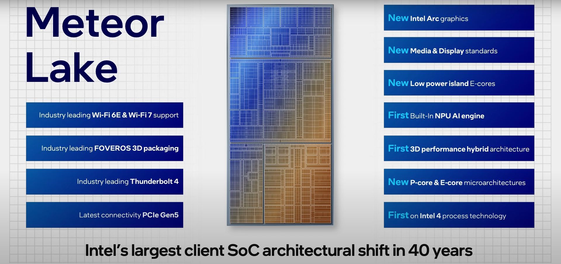
Earlier this year, Intel made a significant move towards streamlining its branding strategy for Core processors, opting for simpler names and bidding farewell to explicit generation numbers like 12th Gen Core or 13th Gen Core. However, the transformation brought about by Meteor Lake goes far beyond mere label adjustments. Intel has undertaken a comprehensive overhaul, encompassing everything from the chip’s physical layout to its underlying architecture. This overhaul introduces a slew of new features, capabilities, and sets the stage for future innovations.
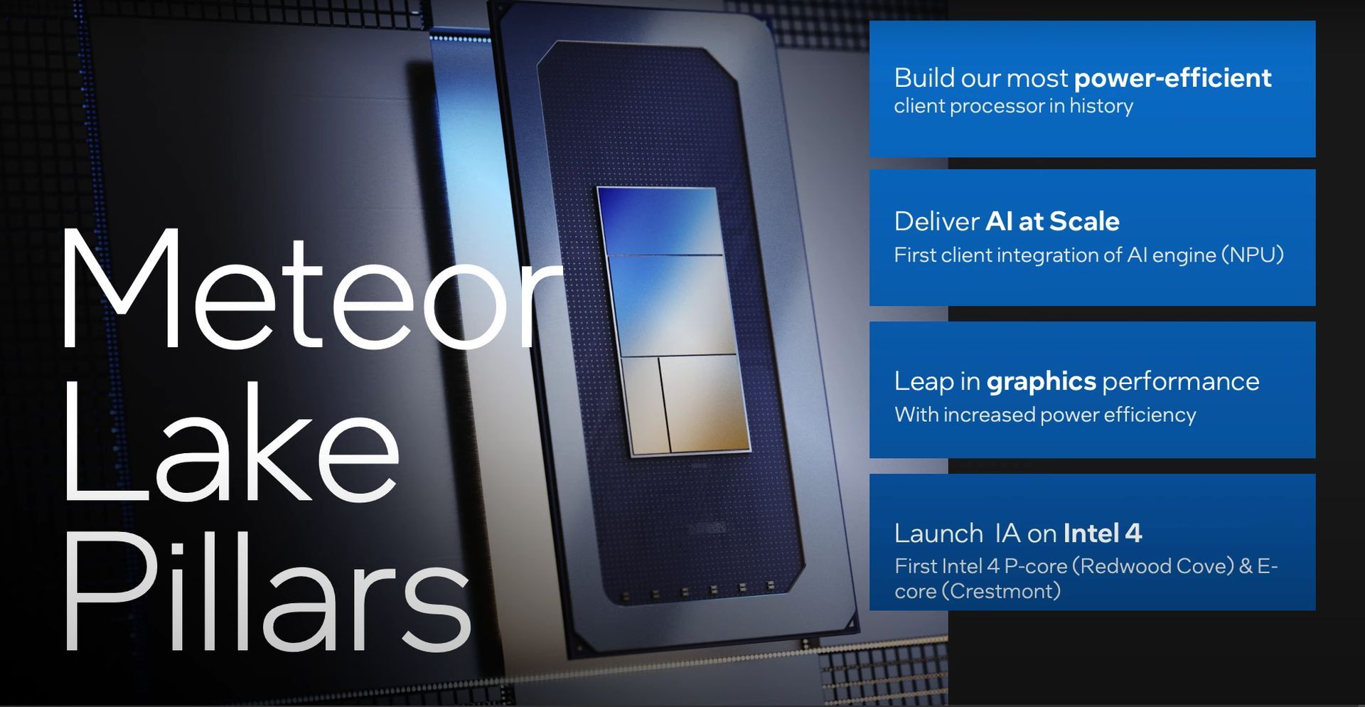
Moreover, Meteor Lake introduces substantial shifts in the manufacturing processes, heralding a reimagined approach with a “stacked” 3D design that integrates various components of the CPU. This innovation dovetails with an expanded emphasis on the tiered approach to processor cores, differentiating between high-power and low-power cores—an approach that gained traction in recent years. Consequently, we are now on the cusp of a redefined Intel processor. This design blueprint is poised to underpin what Intel is likely to christen as the inaugural generation of Intel Core Ultra processors, shedding the iconic “i” for a more straightforward nomenclature.
Intel 4 manufacturing: The 7nm breakthrough
Intel’s significant advancement lies in its transition to the Intel 4 process, a cutting-edge 7-nanometer (7nm) manufacturing technique utilizing extreme ultraviolet (EUV) lithography. This revolutionary method enables the creation of even smaller chips, ensuring Moore’s Law remains on track with increasingly compact transistors.
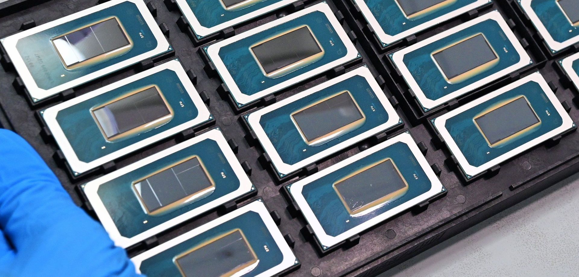
While the EUV lithography equipment is hailed as one of the most intricate machinery ever developed by Intel, the advantages are clear: enhanced scalability and heightened power efficiency. In comparison to the preceding 10nm Intel 7 process, Intel 4 is projected to deliver a notable 20% improvement in performance per watt.
Furthermore, it is finely-tuned for high-performance applications, accommodating both low- and high-voltage operations, providing CPUs with greater adaptability in efficiently managing diverse processes.
Foveros 3D Die Stacking
Intel’s Foveros technology is a cutting-edge packaging solution, utilizing 3D stacking to merge multiple component tiles, also known as “chiplets,” into a single chip. This departure from the monolithic design allows Intel to customize individual parts of the processor, optimizing them for specific functions and creating a compact, efficient 3D stack.
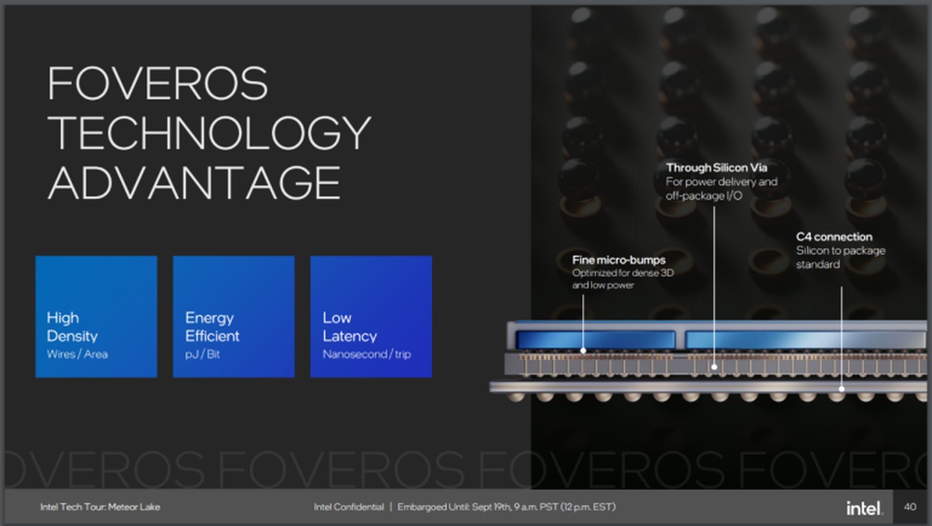
It also enables the use of different production methods for various sections of the chip, leveraging existing manufacturing capabilities. This process refinement eliminates the need for “binning,” a categorization process based on component quality, allowing for a more precise assembly of processors from pre-tested components.
In this new model, Intel can update specific portions of the chip without necessitating a complete redesign. To ensure seamless communication between tiles, specialized die-to-die interconnects are employed, serving as micro-wires for I/O, power delivery, and routing. Intel’s Foveros technology employs high-density, high-bandwidth, and low-power interconnects to unify different parts of the design.
While not an entirely novel approach, this marks a significant shift for Intel, shaping the future of their processor hardware production.
The essence of Intel’s tile layout
The tile-based methodology represents a form of disaggregated design. Instead of creating a single, unified chip, the CPU is constructed from smaller, more straightforward components. These pieces are then assembled onto a base wafer and fused together into a unified chip using the previously mentioned interconnects. However, this Voltron-esque approach necessitates the seamless coordination of multiple components working in tandem.
In the case of Meteor Lake, four distinct tiles will be employed, each specialized for various technologies integral to modern processors: Compute, Graphics, SoC, and I/O.
Compute Tile
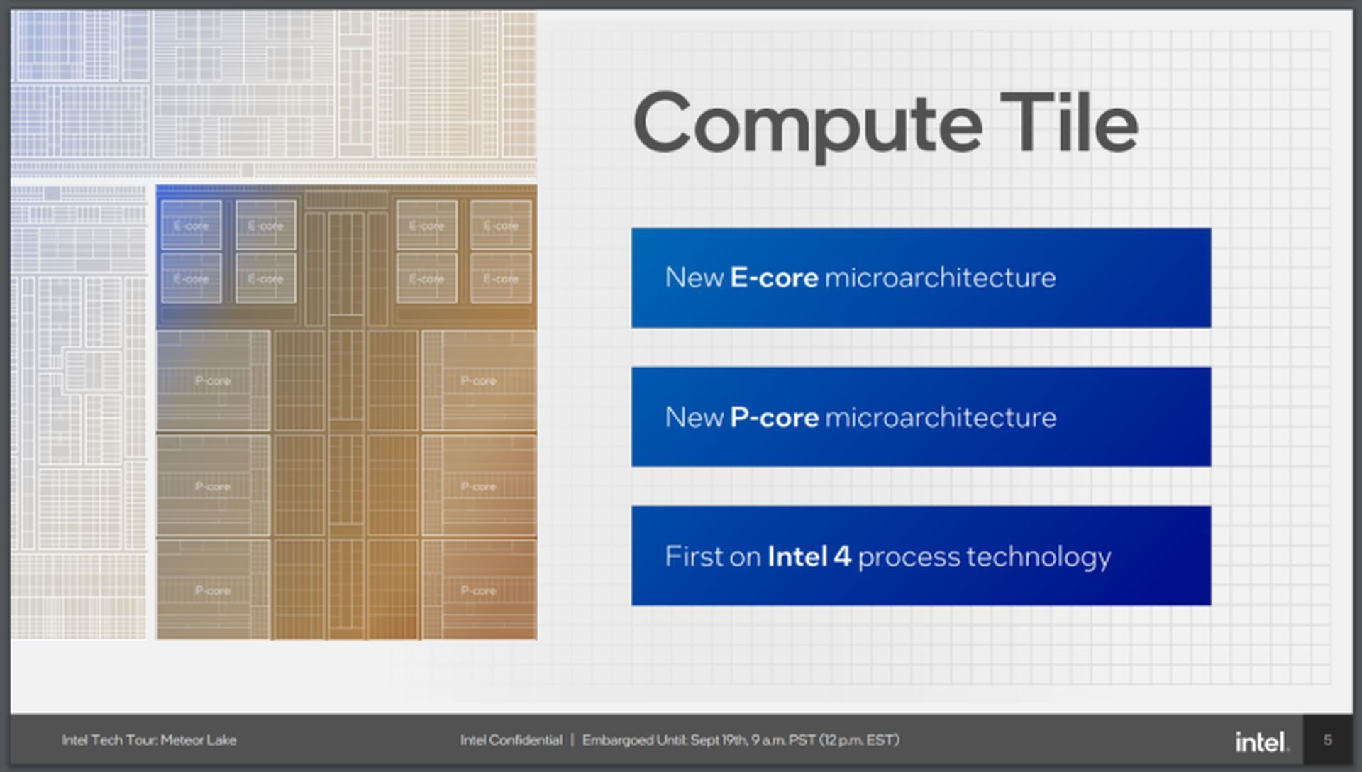
At the core of the Meteor Lake chip lies the Compute Tile, embodying the classic essence of processors. Here, the Performance cores (P-cores) and Efficient cores (E-cores) take charge of the system’s heavy lifting. Utilizing the latest 7nm Intel 4 process, this tile stands as the most advanced among the four.
Intel introduces a new microarchitecture termed “Rosewood Cove” for the P-cores, while the E-cores receive an update with the microarchitecture dubbed “Crestmont.” These enhancements target the optimization of multi-threaded workloads, elevating cache and memory bandwidth, and accelerating AI tasks.
A pivotal component in this process is the Thread Director firmware, an intrinsic feature of previous-gen Intel chips. It ensures that processing tasks are directed to the most suitable core at any given moment. With Meteor Lake, an enhanced Thread Director integrates these cores with refined task-scheduling capabilities and improved guidance. This directs less demanding tasks to the E-cores, and to the new “Low Power E-cores” on the SoC tile (more on these in a moment) for heightened efficiency and power conservation.
This dynamic prioritization reserves the P-cores for high-demand tasks, potentially leading to significant power savings. Intel has also collaborated with Microsoft in redesigning Thread Director, tailoring it closely to Windows 11 for seamless hardware-software integration.
SoC Tile: Melding efficiency with AI prowess
The SoC Tile serves as a versatile hub, overseeing essential functions like media control, display management, Wi-Fi connectivity, and hardware security. It introduces a distinctive feature known as the “Low Power Island,” an isolated zone within the SoC Tile. This area houses efficient processing cores, specifically the Low Power E-cores, tailored for lighter workloads and background tasks. This design enhances overall efficiency while preserving the Compute Tile cores for more demanding applications.
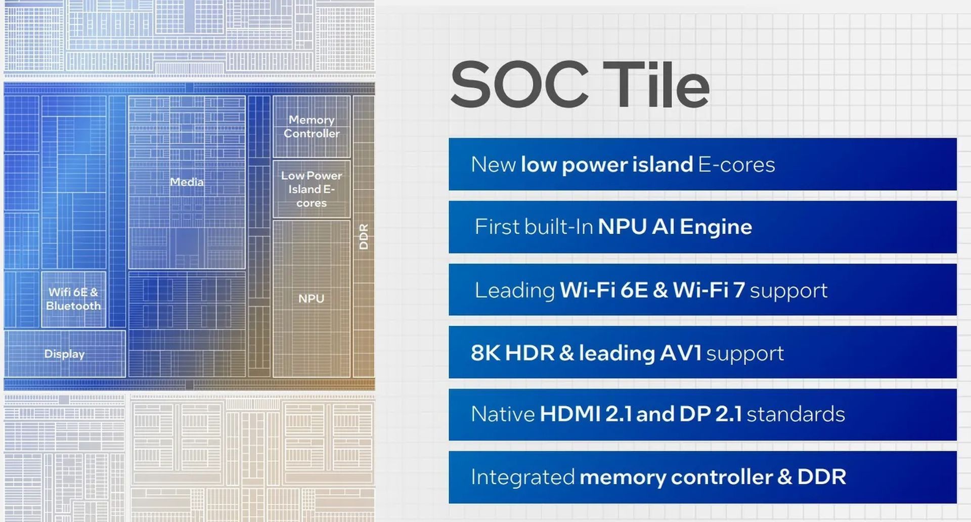
Moreover, the separate power management of the Low Power Island minimizes power overhead, a common occurrence in current CPUs. Tasks that do not require the use of P-cores or E-cores on the Compute Tile can lead to significant power savings by allowing the Tile to remain dormant while the action transpires on the Island.
The SoC Tile integrates Intel’s inaugural integrated artificial intelligence engine—a neural processing unit (NPU) dedicated to efficiently running local AI models. This cooperative effort with the CPU enhances AI workloads, providing high-bandwidth access to various parts of the chip, augmenting everything from graphics to Wi-Fi performance.
In terms of additional functionalities, the SoC Tile includes native HDMI 2.1 and DisplayPort 2.1, supporting features like 8K HDR content and advanced AV1 codecs. It also manages Wi-Fi connectivity, accommodating both current Wi-Fi 6E and upcoming Wi-Fi 7 networking standards. Finally, the SoC Tile houses the memory controller and the double data rate (DDR) bus for seamless communication with system memory.
Graphics Tile: Visual and computational capabilities
The Graphics Tile, the third tile, takes charge of all graphics and compute tasks, including gaming, content creation, and certain media streaming functions. This is where Intel showcases its latest technology: Intel Arc. In this setup, known as Alchemist Xe LPG, the Arc graphics technology is seamlessly integrated into the CPU Graphics Tile. (For in-depth details on Meteor Lake’s new on-chip Arc graphics, click the provided link.)
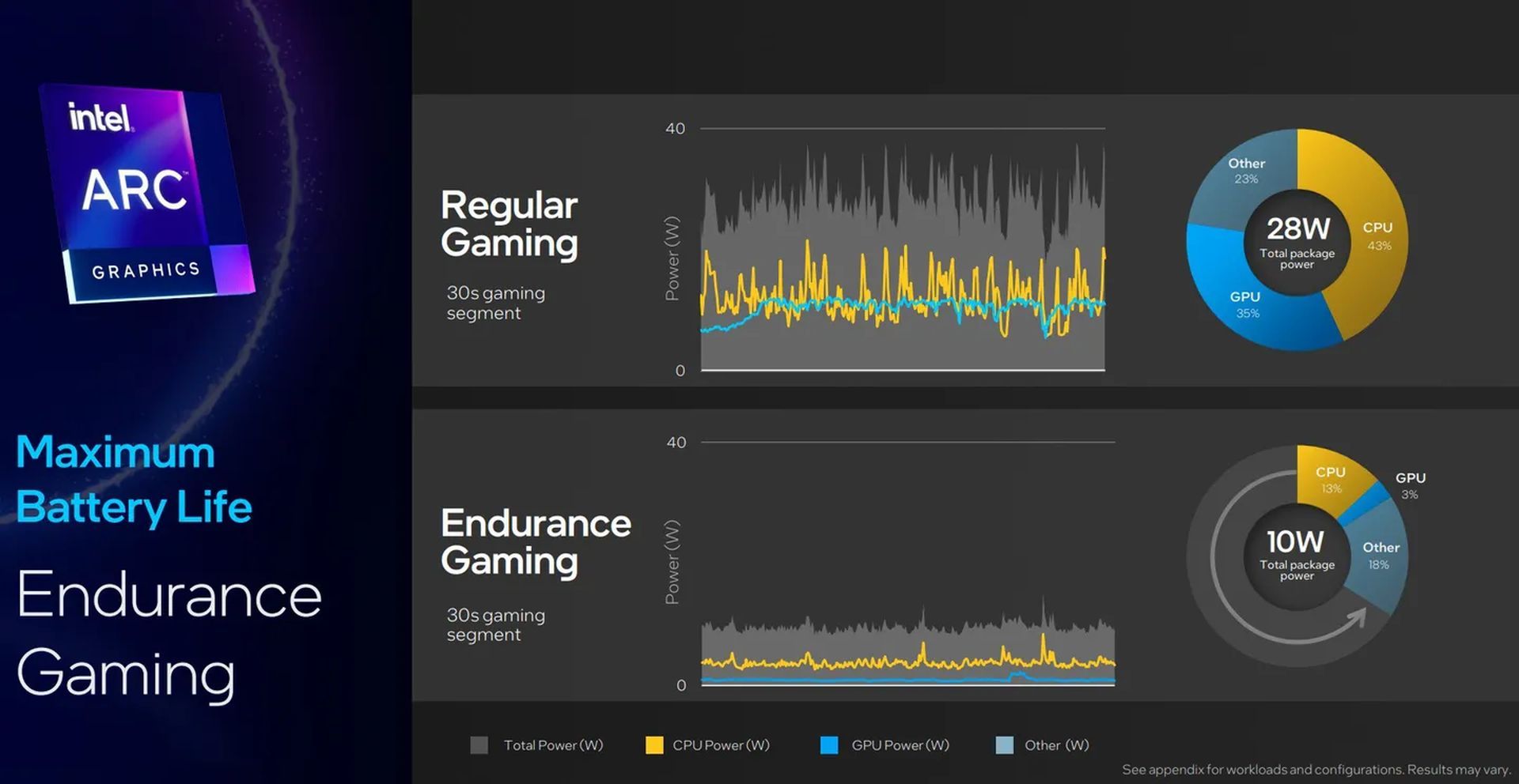
This integration significantly boosts the power and capabilities of Intel’s integrated graphics support. It’s worth noting that this Arc-level performance won’t be available on every Meteor Lake chip, but it marks a substantial advancement beyond Intel’s current Iris Xe solution.
I/O Tile: The nerve center of connectivity
The final segment of the chip focuses on connectivity, managing all pins and signaling for external connections. This encompasses conventional links like USB and storage. Intel has confirmed that the new platform incorporates standards like Thunderbolt 4 and PCI Express Gen 5.
While Intel hasn’t explicitly stated this, we suspect that Thunderbolt 5 support may also be integrated. In a separate briefing dedicated to Thunderbolt 5, Intel announced that the new standard would be launched in 2024. It might be a tad early for Intel to include this new standard in the initial wave of upcoming Meteor Lake chips. However, it wouldn’t be surprising if Thunderbolt 5 is brought up again when Meteor Lake devices are unveiled in the future.
Intel’s chiplet-shaped comeback
Meteor Lake represents a strategic shift for Intel, transcending incremental improvements. It symbolizes Intel’s concerted effort to remain competitive amidst mounting pressures, heralding a new era of potent and versatile laptops.
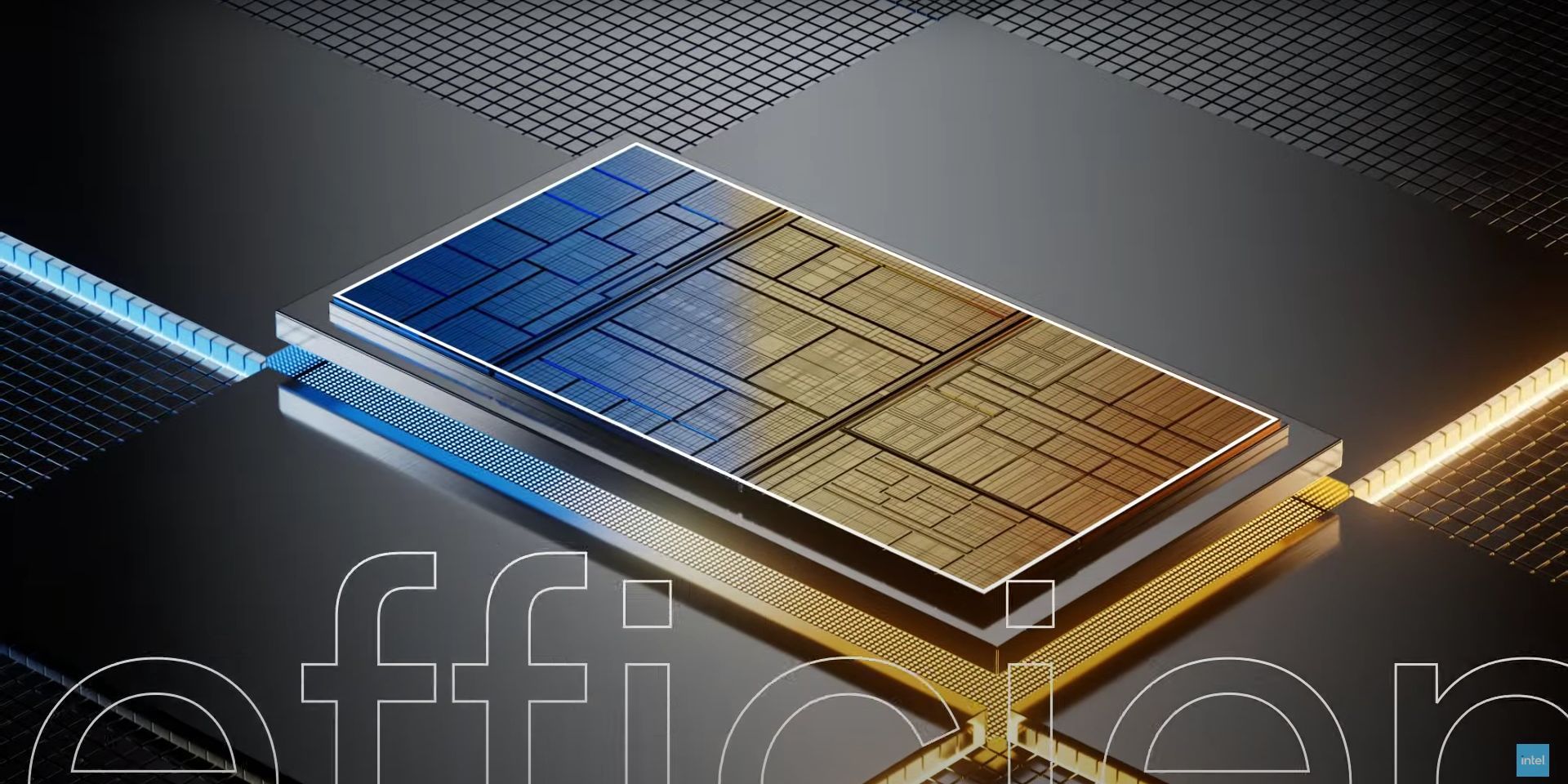
Intel’s Meteor Lake architecture signifies more than a technological evolution; it’s a transformative leap. With its novel approach to tiles, heightened efficiency, and augmented capabilities, it ushers in a new epoch of computing prowess. As we approach the launch of Core Ultra chips on December 14, the industry braces for the arrival of Meteor Lake, poised to redefine computing standards in the near future. CES 2024 holds the promise of unveiling a new era in computing performance and capabilities, as manufacturers gear up to announce their Meteor Lake-powered machines.
Meanwhile, if you are interested in the company’s strategy for the coming years, make sure to check out how the tumbling PC market caused pay cuts in Intel.
Featured image credit: Intel

