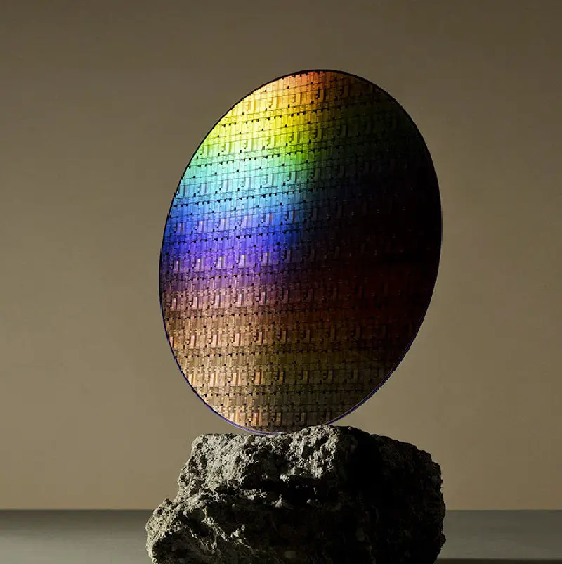
IBM and Samsung have teamed up to create a new semiconductor design, they might have come up with a new way to stack transistors vertically on a chip.
Samsung and IBM reveal a new energy-efficient chip design
Samsung and IBM announced their joint project on the first day of IEDM 2021 and followed it up with a press release. The companies say that they have made new advances in their research in order to create a new semiconductor design.
The companies are working on a new kind of transistor positioning. Transistors are stacked vertically on the chip in the new design. On the current generation of processors, transistors are lying flat on the surface of the semiconductor. This way electricity flow from one side to the other.
The new design is called a Vertical Transport Field Effect Transistor (VTFET). The transistors are stacked in a perpendicular arrangement in the VTFET design so that the electrical current can flow vertically.

Both companies stressed out the potential benefits of the new design. This method should improve the energy efficiency of the system by a substantial margin.
“Overall, the new design aims to deliver a two times improvement in performance or an 85 percent reduction in energy use as compared to scaled finFET alternatives.”
Most importantly, with this new design, Samsung and IBM thinks that “energy intensive processes, such as cryptomining operations and data encryption, could require significantly less energy and have a smaller carbon footprint.”
The companies also made a reference to Moore’s Law in the press release. Moore’s Law is the principle that states that the number of transistors in an IC chip should double about every two years. As a result, performance improves without the chip getting bigger.
However, as the two manufacturers note, engineers are running out of space, and the pursuit of Moore’s Law is becoming more difficult. This new chip design might extend Moore’s Law into the future.


