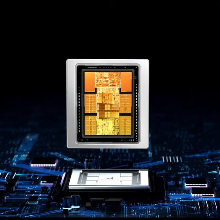
As June 2025 draws to a close, new and significant details have emerged regarding Huawei’s forthcoming Ascend 910D chip, an artificial intelligence (AI) processor poised to potentially rival Nvidia’s advanced System-on-Chips (SoCs). These insights, shared by an X tipster identified as @Jukanlos, shed light on Huawei’s strategic shift towards sophisticated chiplet integration, a move necessitated by current technological limitations and aimed at achieving high-performance computing capabilities.
The core of these recent revelations centers on Huawei’s latest patent, which describes a quad-chiplet design. This architectural approach, where a monolithic chip is segmented into smaller, modular components known as chiplets that are then assembled into a single package, bears a striking resemblance to Nvidia’s established quad-die Rubin Ultra design. If these rumors prove accurate, the Ascend 910D could indeed position Huawei as a formidable competitor in the global AI chip market, directly challenging the technological leadership of the US-based chipmaker, Nvidia.
The adoption of chiplet technology, also referred to as System-in-Package (SiP), represents a crucial evolution in semiconductor manufacturing. This modular method allows for the integration of various smaller SoCs into one cohesive unit, offering enhanced flexibility and efficiency in chip development. When this integration encompasses diverse types of chips within a single package, it is known as heterogeneous integration, a concept Huawei appears to be embracing with its Ascend 910D. This approach contrasts with traditional monolithic chip designs, where the entire integrated circuit is fabricated on a single die. The inherent challenge with larger dies is that an increase in size reduces the number of chips that can be produced from a single semiconductor wafer, thereby decreasing profitability and increasing the impact of manufacturing defects on overall production yield.
A key driver behind Huawei’s intensified focus on chiplet design is the company’s current lack of access to advanced Extreme Ultraviolet (EUV) lithography machines. These state-of-the-art machines are essential for manufacturing the most sophisticated and high-density AI processors with traditional monolithic designs. Without EUV capabilities, Huawei is strategically investing in innovative packaging technologies to circumvent these manufacturing constraints and continue advancing its chip performance.
To further enhance the performance and interconnectivity of its chiplet-based designs, Huawei intends to utilize hybrid bonding. This advanced bonding technique combines copper-to-copper bonding with dielectric bonding, facilitating the creation of high-density, high-performance interconnects crucial for sophisticated 3D device stacking. This method promises superior signal and power delivery compared to conventional interconnect techniques, thereby maximizing the efficiency and speed of data transfer between the individual chiplets within the Ascend 910D.
Interestingly, Huawei appears to be ahead of major industry players like Samsung and Apple in the practical integration of chiplet technology into its products. While both Samsung and Apple are reportedly still in the planning stages, considering the adoption of chiplets for their products by 2026 or 2027, Huawei has seemingly already begun implementing this advanced integration in its current or near-future offerings.
In essence, the recent leaks and patent disclosures strongly suggest that Huawei harbors ambitious plans for its next-generation AI processor, the Ascend 910D. The strategic emphasis on chiplet design, coupled with advanced hybrid bonding techniques, underscores Huawei’s commitment to innovation in the face of geopolitical and technological challenges. The full scope of Huawei’s advancements and the true capabilities of the Ascend 910D will become clearer upon its official market debut, an event eagerly anticipated by industry observers and competitors.


